3.2 Experiment 2
3.2 Experiment 2
3.2 Experiment 2
Important File: Lab 2 Manual
Code Analysis
This experiment is more complex compared to the previous one, involving 6 Verilog files. Let’s first categorize them by hierarchy:
uart_led.vmeta_harden.vuart_rx.vmeta_harden.vuart_baud_gen.vuart_rx_ctl.v
led_ctl.v
This is the design hierarchy for this lab. It can be understood that each .v file calls the module(s) in other .v files, ultimately forming a complete project.
We will analyze it from top to bottom, starting with the uart_led.v file. This top-level file mainly calls modules and passes parameters to integrate UART and LED functionality. You can refer to the code for more details.
The led_ctl.v file defines an LED module that can accept 8-bit data and display it on the LED module.
The main implementation of the code is as follows:
  always @(posedge clk_rx)
  begin
    if (rst_clk_rx)
    begin
      old_rx_data_rdy <= 1'b0;
      char_data       <= 8'b0;
      led_o           <= 8'b0;
    end
    else
    begin
      // Capture the value of rx_data_rdy for edge detection
      old_rx_data_rdy <= rx_data_rdy;

      // If rising edge of rx_data_rdy, capture rx_data
      if (rx_data_rdy && !old_rx_data_rdy)
      begin
        char_data <= rx_data;
      end

      // Output the normal data or the data with high and low swapped
      if (btn_clk_rx)
        led_o <= {char_data[3:0],char_data[7:4]};
      else
        led_o <= char_data;
    end // if !rst
  end // always
In the always @(posedge clk_rx) block, the code is executed every time there is a rising edge on clk_rx. It first checks if (rst_clk_rx) to determine if the module is in a reset state. If it is, then old_rx_data_rdy, char_data, and led_o are all set to 0 (i.e., resetting all states). Otherwise, it proceeds to the else section.
When not in reset state (entering the else block), the first step is to assign the parameter rx_data_rdy (which indicates UART data is ready) using the non-blocking assignment <= to old_rx_data_rdy.
Note that <= is a non-blocking assignment, meaning that the value will be updated only after all always blocks have finished executing!!!
Next, it checks if (rx_data_rdy && !old_rx_data_rdy).
This logic determines if rdy is 1 in the current clock cycle (indicating that RX data is available) while rdy was 0 in the previous clock cycle (indicating no data was available in the previous cycle). If both conditions are true, it means this is new data, and char_data is updated to rx_data (i.e., the UART data).
Note that due to the non-blocking assignment, old_rx_data_rdy is still holding the value from the previous clock cycle during the if check, and hence char_data is updated after the always block completes its execution.
The final part is about displaying the data on the LEDs. It first checks the value of btn_clk_rx (an external button input). If it is 1, the lower 4 bits and upper 4 bits of led_o are swapped. Otherwise, char_data is displayed directly.
Next, let’s explain the purpose of meta_harden.v and uart_baud_gen.v.
The meta_harden.v module mainly implements the function of double synchronization, which aims to synchronize an asynchronous signal into the target clock domain.
Simply put, if the asynchronous signal is a button, the button press is not synchronized with the FPGA clock signal. If it is pressed exactly at the rising edge of the clock, it could result in the button's signal being unstable (metastable), which could cause issues during subsequent reads. This is a common issue with synchronizing asynchronous signals, and thus a double synchronization process is required.
The implementation code is as follows:
  always @(posedge clk_dst)
  begin
    if (rst_dst)
    begin
      signal_meta <= 1'b0;
      signal_dst  <= 1'b0;
    end
    else // if !rst_dst
    begin
      signal_meta <= signal_src;
      signal_dst  <= signal_meta;
    end // if rst
  end // always
Implementing double synchronization is not very complicated. First, it is important to understand the concept of non-blocking assignment mentioned earlier. Specifically, <= operations are only updated after all always blocks have completed execution. In this module, signal_src is first assigned to signal_meta, and then in the next clock cycle, signal_meta is assigned to signal_dst.
Of course, based on this principle, you could implement n-level synchronization by adding more <= assignments as needed, depending on project requirements.
The uart_baud_gen.v module is primarily used to generate the baud rate, focusing on implementing oversampling.
Let's first understand the logical part of it, and then analyze how to determine the frequency count value.
The logical code is as follows:
assign internal_count_m_1 = internal_count - 1'b1;
  always @(posedge clk)
  begin
    if (rst)
    begin
      internal_count  <= OVERSAMPLE_VALUE;
      baud_x16_en_reg <= 1'b0;
    end
    else
    begin
      // Assert baud_x16_en_reg in the next clock when internal_count will be
      // zero in that clock (thus when internal_count_m_1 is 0).
      baud_x16_en_reg   <= (internal_count_m_1 == {CNT_WID{1'b0}});
      // Count from OVERSAMPLE_VALUE down to 0 repeatedly
      if (internal_count == {CNT_WID{1'b0}})
      begin
        internal_count    <= OVERSAMPLE_VALUE;
      end
      else // internal_count is not 0
      begin
        internal_count    <= internal_count_m_1;
      end
    end // if rst
  end // always
First, let's roughly understand the purpose of assign internal_count_m_1 = internal_count - 1'b1;. This is a continuous assignment statement, which is implemented through combinational logic in hardware. When internal_count changes, internal_count_m_1 also changes immediately, without needing clock synchronization.
The always @(posedge clk) block is triggered on every rising edge of the clock (clk). When the module is in reset, internal_count is assigned the value of OVERSAMPLE_VALUE, and baud_x16_en_reg is set to 0.
The above logic implements triggering baud_x16_en_reg after a certain number of clock cycles. For example, if the clock frequency is 1 kHz, and it triggers every 10 cycles, that means it achieves sampling at 100 Hz. If the baud rate is 10 Hz, then it is a 10-times oversampling.
The implementation code is as follows:
  parameter BAUD_RATE    = 57_600;              // Baud rate
  parameter CLOCK_RATE   = 50_000_000;
  // The OVERSAMPLE_RATE is the BAUD_RATE times 16
  localparam OVERSAMPLE_RATE = BAUD_RATE * 16;
  // The divider is the CLOCK_RATE / OVERSAMPLE_RATE - rounded up
  // (so add 1/2 of the OVERSAMPLE_RATE before the integer division)
  localparam DIVIDER = (CLOCK_RATE+OVERSAMPLE_RATE/2) / OVERSAMPLE_RATE;
  // The value to reload the counter is DIVIDER-1;
  localparam OVERSAMPLE_VALUE = DIVIDER - 1;
  // The required width of the counter is the ceiling of the base 2 logarithm
  // of the DIVIDER
  localparam CNT_WID = clogb2(DIVIDER);
This part is used to calculate the value of OVERSAMPLE_VALUE, which determines how many clock cycles are required to trigger baud_x16_en_reg each time, as mentioned above.
Subtracting 1 is because the counter starts from 0.
The purpose of clogb2(DIVIDER) is to calculate the number of bits needed to represent DIVIDER in binary. This ensures an appropriate counter width, which can help save resources.
The implementation code is as follows:
  function integer clogb2;
    input [31:0] value;
    reg   [31:0] my_value;
    begin
      my_value = value - 1;
      for (clogb2 = 0; my_value > 0; clogb2 = clogb2 + 1)
        my_value = my_value >> 1;
    end
  endfunction
The main logic is to keep right-shifting value until it becomes 0, and for each shift operation, clogb2 is incremented by 1. Finally, the resulting clogb2 represents the number of bits required to represent value in binary.
Finally, let's discuss the purpose of uart_rx.v and uart_rx_ctl.v.
The uart_rx.v module primarily calls other modules and passes parameters, similar to what uart_led.v does.
The main focus is on uart_rx_ctl.v, which is responsible for implementing a UART receiver controller that receives UART data and decodes it.
This part of the code is quite long, with detailed comments, so here we will briefly explain its purpose. Please refer to the code for specific details.
There are five always blocks that run concurrently, and we will refer to them as Module X in the following explanations.
Module 1implements a state machine function, updating the state at each rising edge of the clock cycle.Module 2checks if data is available, and then reads the current bit's value on the eighth oversampling cycle. Subsequent readings occur every 16 oversampling cycles, starting from the middle of the start bit. This helps ensure stability and prevents issues from unstable data.Module 3is responsible for tracking the number of bits read so far.Module 4checks if the correct number of bits have been read and generates therx_data_rdysignal.Module 5is used for stop bit verification. Normally, the stop bit should be1. If it is not, this indicates a data error, which is communicated through thefrm_errsignal.
It is important to note that all of these always blocks execute concurrently, meaning they all start executing simultaneously on the rising edge of the clock (they use the data from the previous clock cycle).
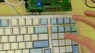
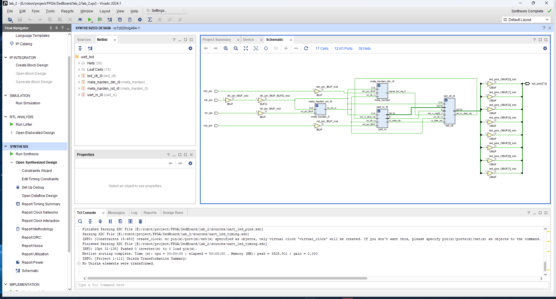
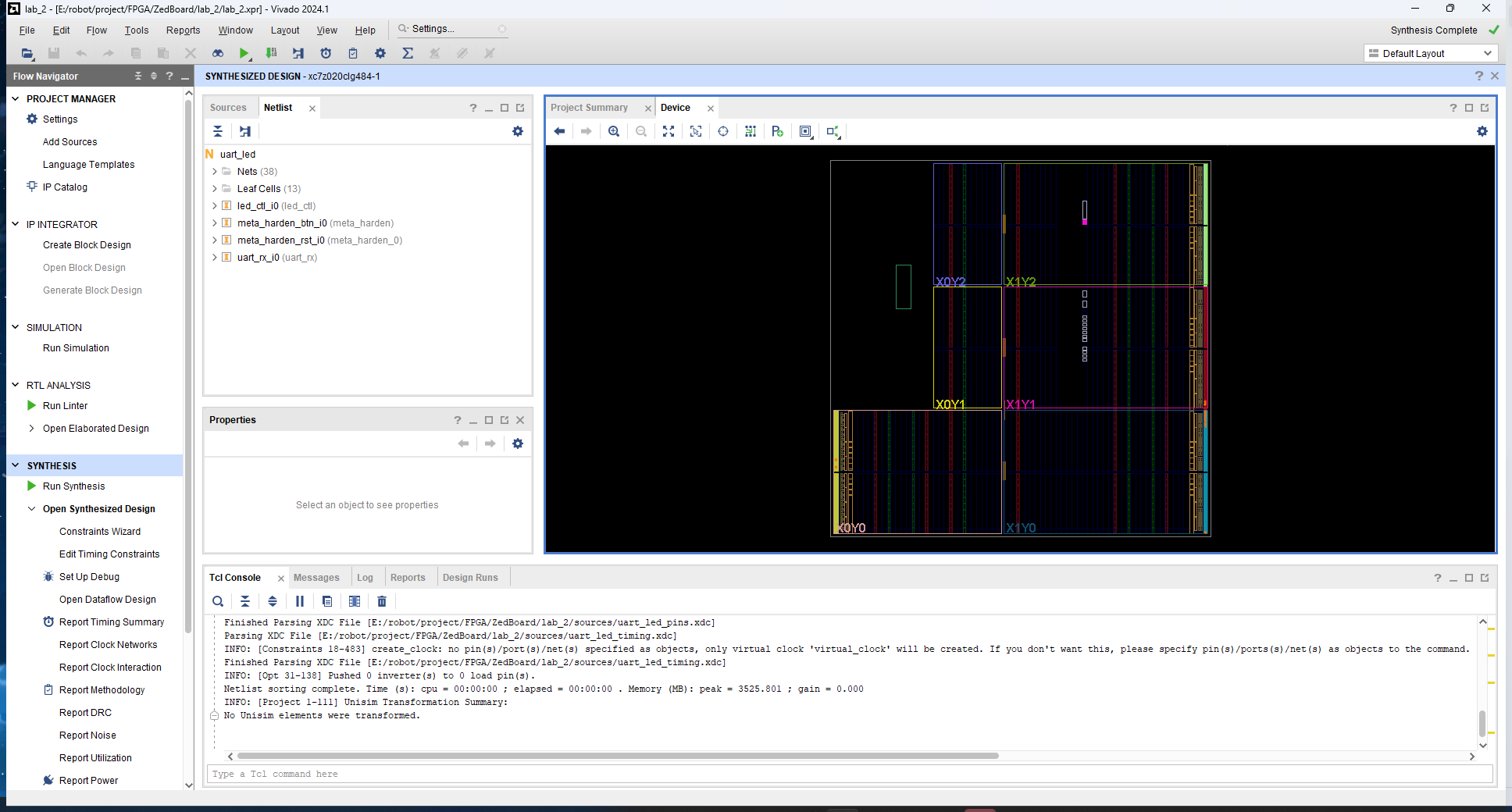
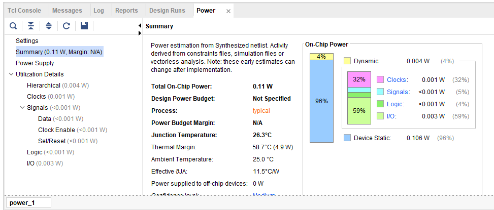
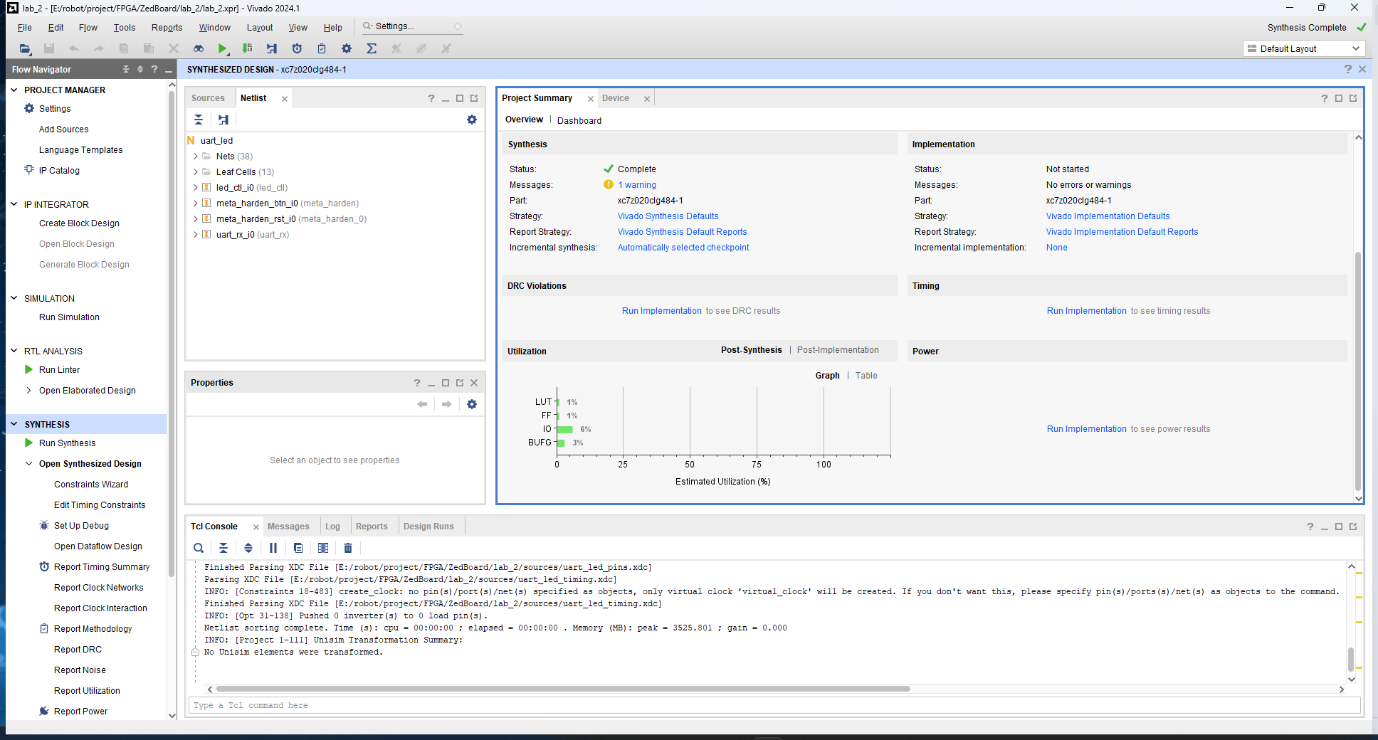
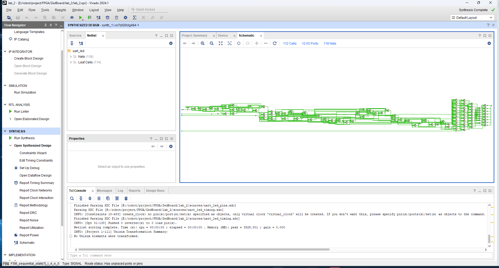
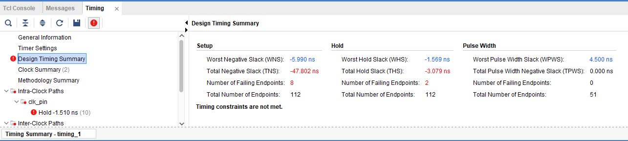
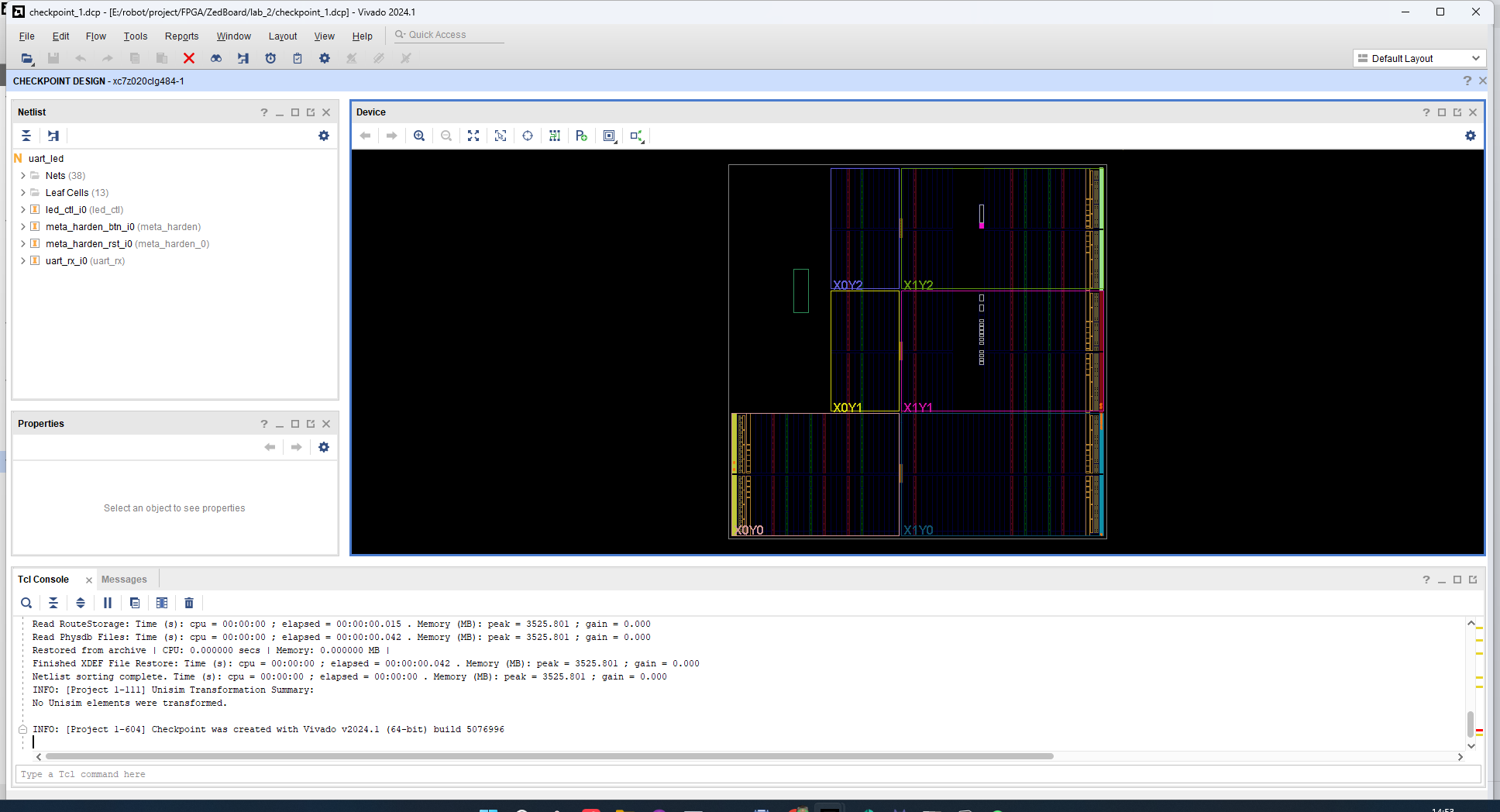
Experimental Results
The following images and animations show the results of the experiment:
Pre-Optimization Schematic
Device View
Power Report
Project Summary
Post-Optimization Schematic
Timing Analysis Report (with Timing Violations)
Checkpoint File
Final Test