3.1 Experiment 1
3.1 Experiment 1
3.1 Experiment 1
Important Document: Lab 1 Manual
Code Analysis
Below is the code for the lab1 module (available in lab1.v), which is mainly used to control the LED display on the ZedBoard. Each LED is controlled by the corresponding switch position. The specific logic is as follows:
The simulation code is similar and is not described here in detail; please refer to it directly.
led[0]corresponds to the inverted value ofswt[0].led[1]is controlled by the combination logic ofswt[1]andswt[2].led[2]andled[3]are also based on different combinations of switches.led[7:4]directly correspond toswt[7:4], meaning these LEDs directly show the state of the corresponding switches.
The code implementation is as follows:
module lab1(
    input [7:0] swt,
    output [7:0] led
    );

    assign led[0] = ~swt[0];
    assign led[1] = swt[1] & ~swt[2];
    assign led[3] = swt[2] & swt[3];
    assign led[2] = led[1] | led[3];

    assign led[7:4] = swt[7:4];
endmodule
The pin constraint file lab1.xdc is used to connect the switches and LEDs to the physical pins on the ZedBoard. Below is the content of the constraint file:
Since XDC files usually involve a lot of repetitive operations, we provide an example for one LED and one switch. The rest of the logic is similar.
set_property PACKAGE_PIN: This command is used to map a logical port (e.g.,swt[0]orled[0]) to a physical pin on the ZedBoard. In this example,swt[0]is assigned to pinF22, whileled[0]is assigned to pinT22.set_property IOSTANDARD LVCMOS33: This command specifies the input/output standard for the pin. Here, we useLVCMOS33, which is a common voltage level standard indicating that the pin operates at a 3.3V logic level.
The code implementation is as follows:
set_property PACKAGE_PIN F22 [get_ports swt[0]]
set_property IOSTANDARD LVCMOS33 [get_ports swt[0]]

set_property PACKAGE_PIN T22 [get_ports led[0]]
set_property IOSTANDARD LVCMOS33 [get_ports led[0]]
Experimental Results
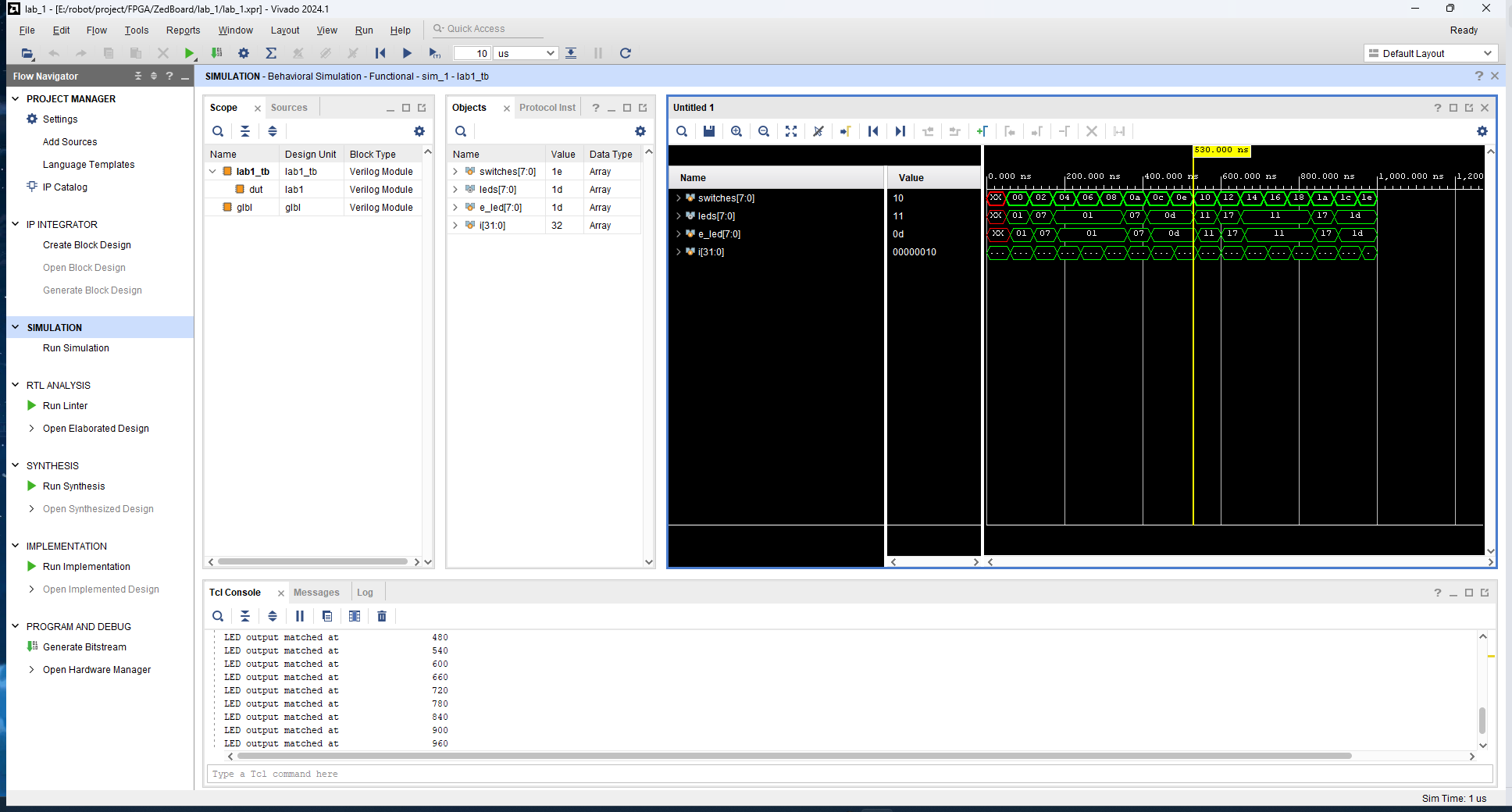
The following images and animations show the results of the experiment:
Behavioral Simulation
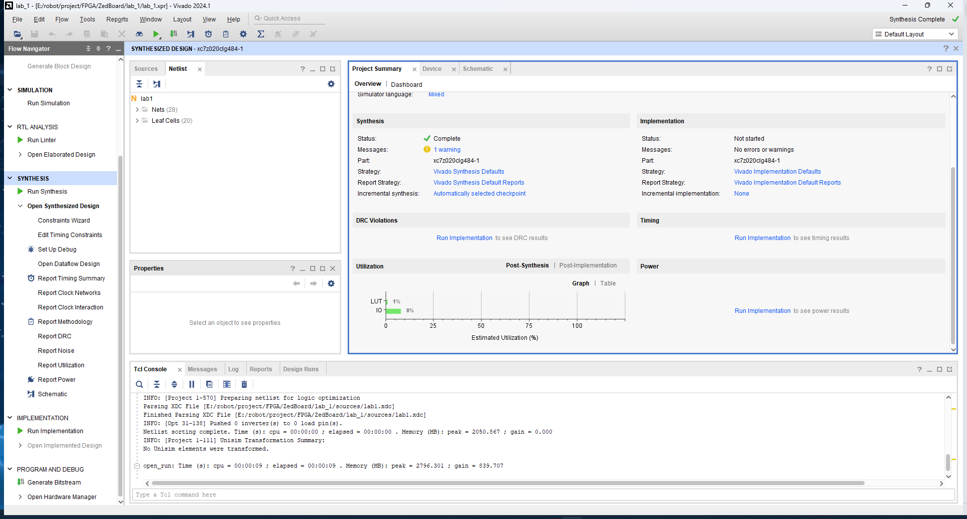
Project Summary
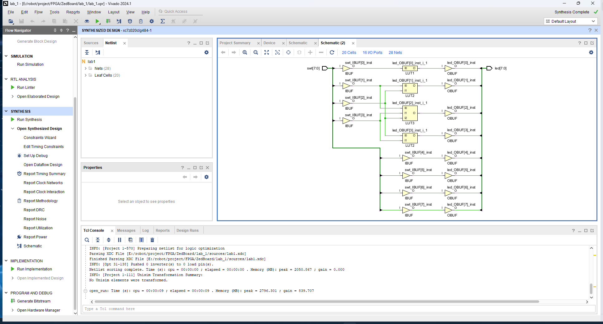
Schematic After Synthesis
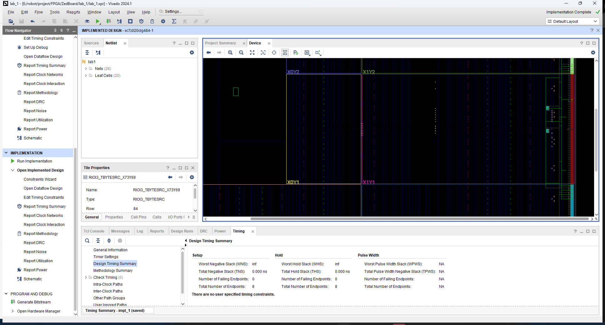
Device Implementation
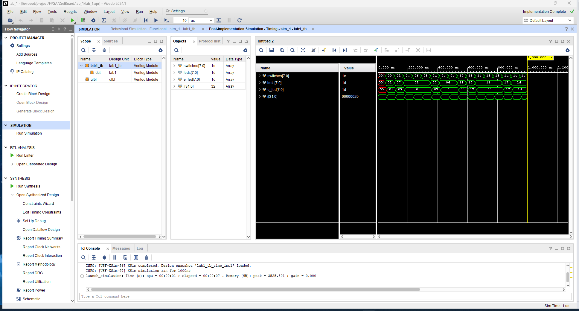
Post Timing Simulation
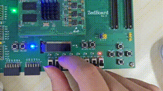
Final Test